Tanmay's Design Study
Tanmay Bhola (Talk | contribs) (→Design Detail) |
Tanmay Bhola (Talk | contribs) |
||
| Line 36: | Line 36: | ||
== Design Detail == | == Design Detail == | ||
| − | The focus was to make the design simple and extensible. Most of the classes map to the requirements discussed in the previous section. | + | The focus was to make the design simple and extensible. Most of the classes map to the requirements discussed in the previous section. The design [[model the real world| models the real world]]. |
| + | |||
| + | * '''Component and Ports''': The component represents a functional block in the circuit. Every component has at least one port to interact with the rest of the circuit. Ports could be input ports or output ports. Components could be in the form of simple logic gates (and/or/xor/nand) or a combination of these forming more complex components (like adders). To represent this part-whole heirarchy of components, the Composite pattern was used in the design. | ||
| + | |||
| + | * '''Wire''' : As described above, a wire is a container for a logic signal and links the output of one component to the input of another. As the signal propagates along the circuit, various events are generated to update the state of the wire after a certain delay interval. The user assigns a name to the wire on creation which can be used for generating the simulation results. The [[Observer| observer pattern]] was used to assist the wire in informing the connected ports about the change in its state. | ||
| + | |||
| + | * '''Event''': | ||
Revision as of 02:36, 30 September 2010
Contents |
Introduction
Welcome to the world of Digital Logic. Ever wondered what they teach at the College of Engineering that is different from the material taught at Department of Computer Science and Software Engineering ? Being a computer engineering student, I took this opportunity to perform Object-Oriented Analysis and Design of a 'Digital Logic Circuit Simulator'. Digital Circuits are constructed by joining simple logic elements and form the basis of our 'Embedded Systems' oriented programme. The system was designed and implemented specially for COSC427, and was not a part of another university project.
Background
Building complex digital structures like computers and microcontrollers without a simulation tool is similar to releasing a program without compiling/testing. Hence, designers always resort to simulation tools to check the correctness of their design before building the prototype. These circuits are essentially complex networks of simple logic components like logic gates, wires, clocks etc.
A digital logic simulator gives the user an ability to join simple logic elements in order to study the behaviour of complex digital circuits. My approach to this problem was to design an 'Event Driven Simulator' where events (change in state of something) trigger further events in the system at a later time. The main tasks revolved around the elementary components of the circuit and scheduling events that take place in the system. These can be further broken down into :
- 1) Wires --- These carry digital logic signals between components and have state associated with them.
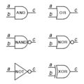
- 2) Digital Function Blocks --- These perform functions to generate output signal(s) based on input signal changes. They need to listen for changes in the state of wires connected to the inputs of these blocks. An example of a function block is an and logic gate. It performs the bitwise AND function ( X = A.B) over inputs A and B.
- 3) Events --- The simulation is purely event based. This means that changes in the state of a wire can lead to generation of various events in the system. These contain a timestamp of execution along with the associated component.
My primary focus for this design study was on modelling the core classes of the simulator rather than its GUI implementation. The aim was to design a system that modelled the real world and could be extended in the future to incorporate GUIs and more components/ modelling techniques.
Requirements
- 1) Adding components : A User should be able to add new components to the system. These components can be a basic logic element or a combination of a series of elements. The user should also be able to copy simple elements in order to quickly build up a circuit. This is useful as many basic elements like logic gates are repeated in the circuit.
- 2) Connecting components with wires : A user should be able to assign connecting wires to the component input/ output ports. On connection, the component should be ready to respond to changes in the state of the wire.
- 3) Scheduling events: Timing is crucial in a digital logic simulation. This makes scheduling events an important task for this 'event driven' simulation software. Function blocks generate events with variable time delays (also known as propagation delays). These need to be executed by the system in the correct order, else the final output of the simulation would be incorrect.
- 3) Running the simulation and viewing results : Once the circuit has been wired up, a user should be able to run the simulation and view the results of the simulation. At this point, a basic text based output with timing information was sufficient. However, a GUI output (showing a graph) might be desired in the future.
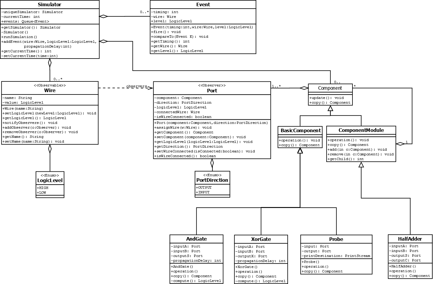
UML Diagram Of Design
Design Detail
The focus was to make the design simple and extensible. Most of the classes map to the requirements discussed in the previous section. The design models the real world.
- Component and Ports: The component represents a functional block in the circuit. Every component has at least one port to interact with the rest of the circuit. Ports could be input ports or output ports. Components could be in the form of simple logic gates (and/or/xor/nand) or a combination of these forming more complex components (like adders). To represent this part-whole heirarchy of components, the Composite pattern was used in the design.
- Wire : As described above, a wire is a container for a logic signal and links the output of one component to the input of another. As the signal propagates along the circuit, various events are generated to update the state of the wire after a certain delay interval. The user assigns a name to the wire on creation which can be used for generating the simulation results. The observer pattern was used to assist the wire in informing the connected ports about the change in its state.
- Event:
Modelling Components using the Composite Pattern
Components could be in the form of simple logic gates (and/or/xor etc.) or a combination of these forming more complex components. The first pattern that comes to mind when thinking about part-whole hierarchies is the Composite Pattern. Hence, this pattern will be used for modelling the components as a start. A high level interface would be used to hide the complexity of individual components and encourage programming to the interface, not the implementation.
Lower level components should be able to take in wires as their inputs and outputs to help with wiring up the circuit.
Modelling a Wire
A wire is essentially a link between two components, and carries (holds) a '1/0' value at any time. The outputs of components SET the value of the view while this change in the value triggers events in components via their inputs. The Observer pattern might be helpful in notifying a subset of components in the circuit (observers !!! ) when the value of the wire changes. Hence the components also implement the <<observer>> interface and can subscribe to changes in the status of the wires connected at their inputs. On receiving such changes, they can recalculate the output values (using the function they implement) and update the output wire status.
Patterns and Principles
Discussion and Design Critique
1) The Composite Design Pattern: No-Op Overrides Vs Dependency Inversion Principle
2) Push Vs. Pull Configuration of the Observer


